| PIN |
|
description |
| CK, /CK |
DDR |
Differential System Clock |
| CKE |
|
Clock enable |
| /CS |
|
Chip Select (active low) |
| /RAS |
|
Row Address Strobe (active low) |
| /CAS |
|
Clolumn Address Strobe (active low) |
| /WEd |
|
Write enable (active low) |
| A0 ... A12 |
|
Address Input |
| BA0 ... BA1 |
|
Bank Address Input |
| DM0 ... DM3 |
|
Input Data Mask |
| DQS0 ... DQS3 |
|
Data Strobe |
| DQ0 ... DQ31 |
|
Data Input/Output |
| Vdd |
|
Power Supply |
| Vddq |
|
Data out Power |
| Vss |
|
Ground |
| Vssq |
|
DQ Ground |
| /CE |
NAND |
Chip enable (active low) |
| /RE |
|
Read enable (active low) |
| /WP |
|
Write protection (active low) |
| /WEn |
|
Write enable (active low) |
| ALE |
|
Address Latch enable |
| CLE |
|
Command Latch enable (command provided via IO0...IO7 and latched on
rising edge of /WE) |
| R /B |
|
Ready/Busy output (chip busy writing when low, can be read when high) |
| IO0 ... IO7 |
|
Data input/output |
| Vcc |
|
+3.3V Power Supply |
| Vss |
|
Ground |
| NC |
- |
not connected |
| DNU |
|
do not use |
 3.1.1.2
TA-080
3.1.1.3
TA-081
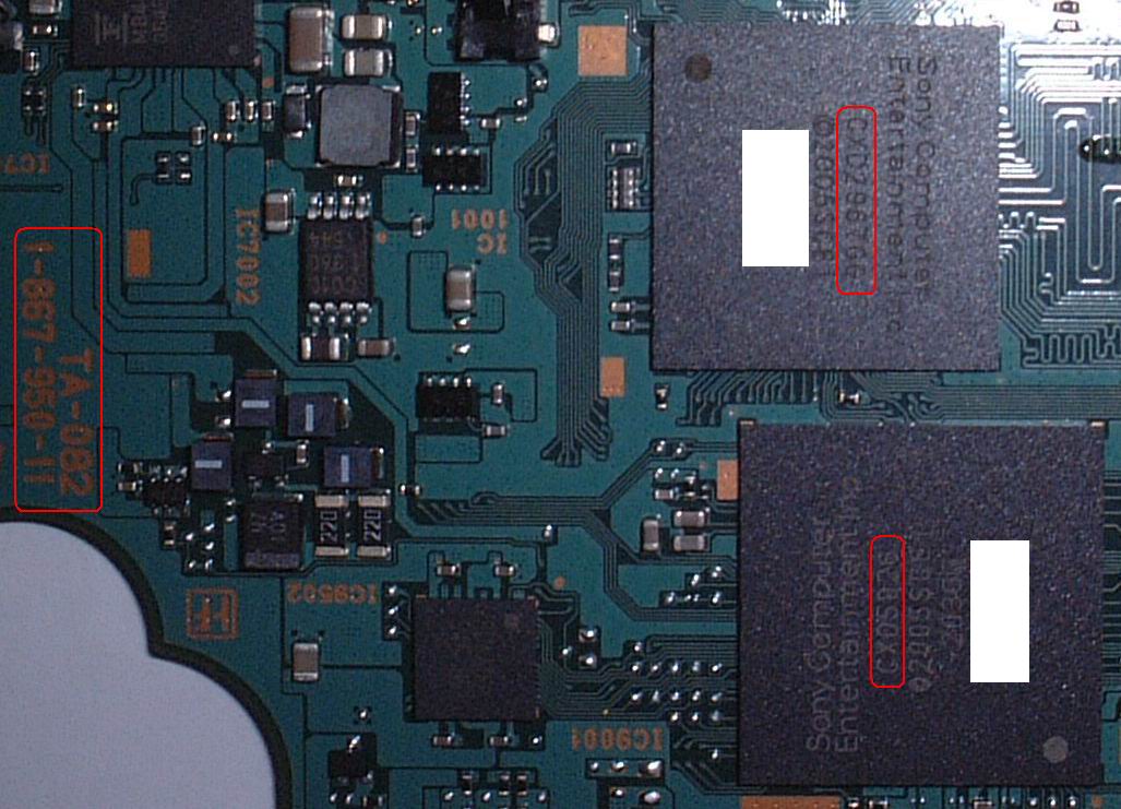
3.1.1.4
TA-082
CPU Core : CXD2967GG
Media Engine : CXD5026-203GG
Flash/SDRAM: K5E5658ACM-D060 (1.8V/1.8V)
3.1.1.2
TA-080
3.1.1.3
TA-081
3.1.1.4
TA-082
CPU Core : CXD2967GG
Media Engine : CXD5026-203GG
Flash/SDRAM: K5E5658ACM-D060 (1.8V/1.8V)
 You can identify this Motherboard by opening the UMD door and looking
for the IC1003 label:
You can identify this Motherboard by opening the UMD door and looking
for the IC1003 label:
 3.1.1.5
TA-086
CPU Core : CXD2967GG
Media Engine : CXD5026-203GG
MCP : K5E5658ACM-D060 1.8V/1.8V
3.1.1.5
TA-086
CPU Core : CXD2967GG
Media Engine : CXD5026-203GG
MCP : K5E5658ACM-D060 1.8V/1.8V


